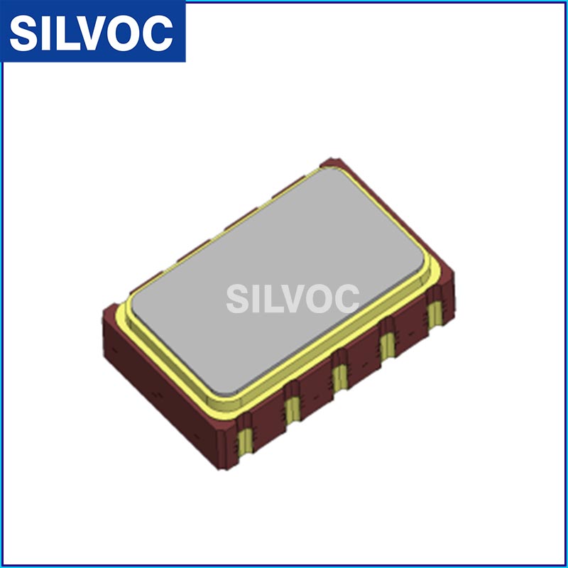
XV7181BB: EPSON High-precision Yaw sensor (Digital Output)
Low angle random walk 0.065 °/√ h Typ.
Supports SPI/I2C serial interface
Built in selectable digital filters
Angular velocity output (16 bit or 24 bit)
Built in temperature sensor
Power supply voltage: 2.7V~3.6V
Working temperature: -40 ° C to+85 ° C
Low power 1.2mA Typ.
Detection range ± 460 °/s, ± 115 °/s
XV7181BB: EPSON High-precision Yaw sensor (Digital Output)

P/N | Q-Code | Size | MOQ |
XV7181BB | X2A000401100200 | 5.0 x 3.2 | 2000PCS/REEL |
XV7181BB 51.000kHz F | X2A000401100200 | 5.0 x 3.2 | 2000PCS/REEL |
The XV7181BB has superior performance characteristics especially with bias output stability and low noise. Epson achieves these performances by using Epson’s original quartz sensor element.
This sensor has digital output interface (SPI and I2C) that is compatible with various interface logic levels enabled by interface power supply voltage settings (VDDI) that are independent of the main power supply voltage (VDDM).
In addition, user-selectable low-pass filters and high-pass filters are available for wide range of cut-off frequencies. The XV7181BB is suitable for various applications from consumer electronics such as wearable devices to industrial equipment.
Low angle random walk 0.065 °/√ h Typ.
Supports SPI/I2C serial interface
Built in selectable digital filters
Angular velocity output (16 bit or 24 bit)
Built in temperature sensor
Power supply voltage: 2.7V~3.6V
Working temperature: -40 ° C to+85 ° C
Low power 1.2mA Typ.
Detection range ± 460 °/s, ± 115 °/s
· Anti-vibration and attitude control for industrial applications etc.
· Autonomous driving equipment such as AGVs and lawn mower
*The I2C-Bus is a trademark of NXP Semiconductors
Gyro Sensor Characteristics
(VDDM = 2.7 V to 3.6V, VDDI = 1.65 V to 3.6 V, GND = 0 V, TOPR = -40 °C to +85 °C)
Item | Symbol | Specifications | Conditions / Remarks |
Supply Voltage | VDDM | 2.7 to 3.6 V | |
Supply Voltage for interface | VDDI | 1.65 V to 3.60 V | |
Storage temperature | TSTG | -40°C to +105°C | |
Operating temperature | TOPR | -40°C to +85°C | |
Scale Factor | So | 264 LSB/(°/s), 66 LSB/(°/s) ±2.0% | 16bit, Ta=+25°C,FS = 1, FS = 1/4 |
67584 LSB/(°/s), 16896 LSB/(°/s) ±2.0% | 24bit, Ta=+25°C,FS = 1, FS = 1/4 | ||
Scale Factor variation over temperature | Spt | ±3.0% | VDDM=3V, Ta=+25°C reference |
Bias | ZRL | ±1 °/s (0 LSB Typ.) | Ta=+25°C |
Bias variation over temperature A | ZRLta | ±0.3 °/s | -10°C to +50°C, Ta=+25°C reference |
Bias variation over temperature B | ZRLtb | ±1.0 °/s | -40°C to +85°C, Ta=+25°C reference |
Bias temperature coefficient | ZRLs | 0.0024 ( °/s)/°C Typ. | VDDM=3V, Average of absolute value, △T=1°C. |
Rate range | I | ±115 °/s, ±460 °/s | FS=1, FS=1/4 |
Non-linearity | NI | ±0.25 %FS | Ta=+25°C |
Cross-axis sensitivity | CS | ±5 % | Ta=+25°C |
Current consumption | Iop1 | 1.4 mA Max. | Not communicating |
Sleep current | Iop3 | 1 μA Typ. | |
Noise density | Nd | 0.0015 (°/s)/√Hz | at 10Hz,LPF Default setting |
Angle random walk | ARW | 0.065 °/√h | |
Bias Instability | Bs | 0.9 °/h Typ. | Bottom value of Allan deviation |
Parameter | Symbol | Conditions | Min. | Type. | Max. |
Supply Voltage | VDDM | 2.7 to 3.6 V | 2.7V | 3.0V | 3.6V |
Supply Voltage for interface | VDDI | 1.65 V to 3.60 V | 1.65V | - | 3.60V |
Storage temperature | TSTG | -40°C to +105°C | -40°C | - | +85°C |
Operating temperature | TOPR | -40°C to +85°C | -40°C | - | +85°C |
Drive frequency | Fd | Frequency code J | 50.450KHz | 51.025KHz | 51.600KHz |
Detuning frequency | Df | 0.7 KHz | 0.9 KHz | 1.1 KHz | |
Scale Factor | So | 16bit, FS = 1x setting | 264 LSB/(°/s) | - | |
16bit, FS = 4x setting | 66 LSB/(°/s) | - | |||
24bit, FS = 1x setting | 67584 LSB/(°/s) | ||||
24bit, FS = 4x setting | 16896 LSB/(°/s) | ||||
Scale Factor tolerance | Sp | Ta=+25°C | -2% | - | +2% |
Sp | Ta=+25°C The value includes after the shipment. | -4% | - | +4% | |
Scale Factor variation over temperature | Spt | VDDM=3V, Ta=+25°C reference | -3% | - | +3% |
Bias | ZRL | Ta=+25°C | - | 0 LSB | - |
Bias tolerance | ZRL | Ta=+25°C | -1 °/s | - | +1 °/s |
Ta=+25°C The value includes after the shipment. | -2 °/s | - | +2 °/s | ||
Bias variation over temperature | ZRL | VDDM = 3 V, Ta = +25 °C reference | -1 °/s | - | +1 °/s |
Rate range | I | FS = 1x setting | -115°/s | +115°/s | |
FS = 4x setting | -460°/s | +460% | |||
Non-linearity | NI | -0.25%FS | +0.25%FS | ||
Cross-axis sensitivity | CS | Ta=+25°C | -5% | +5% | |
Current consumption | Iop1 | - | 1150μA | 1400μA | |
Sleep current | Iop3 | - | 1μA | 30μA | |
Noise density | Nd | - | 0.0015 (°/s)/√Hz | - |
Temperature Sensor Characteristics
(VDDM = 2.7 V to 3.6V, VDDI = 1.65 V to 3.6 V, GND = 0 V, TOPR = -40 °C to +85 °C)
Parameter | Symbol | Condition | Min. | Type. | Max. | Unit |
Output code | Tout | Format 1: Ta = + 25 °C | 2560 | 3200 | 3840 | LSB |
Format 2: Ta = + 25 °C | -1280 | 0 | 1280 | |||
Temperature error | Tacc | Ta = +25 °C | -5 | - | +5 | °C |
Temperature coefficient | Tits | Format 1: Ta = + 25 °C | 115.2 | 128 | 140.8 | LSB/°C |
Format 2: Ta = + 25 °C | 230.4 | 256 | 281.6 |

Detecting Axis and Output Polarity
This product detects an angular rate of a rotational movement. The correlation between a detecting axis of the angular rate and an output polarity is shown in Figure 2.

Figure 2 Detecting Axis and Output Polarity
Interface
This product is compatible with SPI (4-wire, 3-wire) and I2C. This sensor allows for interface power supply
voltage settings (VDDI) that are independent of the power supply voltage (VDDM) to enable communications with
interfaces of various logic levels.
Angular Rate Output
The angular rate output data is provided in the 2’s compliment expression. 16 bits or 24 bits can be selected
from the register settings. The AD converter sampling frequency fs is 12.000 kHz for frequency symbol J.
The angular rate output data can also be provided after processing through the low-pass filter (LPF). In
addition, the Notch Filter (NF) is available and can be enabled to suppress residual output of detuning frequency
after mechanical shock. Regarding the Digital Filter, See the Chapter 8.
LPF: This is a 2nd, 3rd or 4th order filter, the cutoff frequency can be selected.
(1/10/25/50/100/200/400/500 [Hz])
NF: Either enable or disable can be selected. The center frequency of the Notch Filter is already set at our
factory individually.
Temperature Sensor Output
Temperature output data is provided in the 2’s compliment expression. The temperature output in the zero
code can be selected by the register setting. See the Sector 6.5.
P/N | Q-Code | Size | MOQ |
XV7181BB | X2A000401100200 | 5.0 x 3.2 | 2000PCS/REEL |
XV7181BB 51.000kHz F | X2A000401100200 | 5.0 x 3.2 | 2000PCS/REEL |
Product Name
XV7181BB 51.000KHz F
(Standard form) ① ②③④ ⑤ ⑥
① Model ② Detection axis(1:Z-axis) ③ Package type (B : Ceramic 5.0 x 3.2 mm )
④ Output (B: SPI / I2C) ⑤ Frequency ⑥Custom recognition (not necessary to specify)
Product Number
XV7181BB 51.000KHz F X2A000401100200
① ② ③ ④ ⑤
① Crystal devices ② Model
③ Pb free code(1 or 2: EU RoHS compliant / Pb free)
④ Detail specifications ⑤ Packing code (00: Standard : 2000pcs/Reel)
*Blank section is decided by each detail specification.


Pin number. | Pin name | Input/Output | Pin description |
#1 | MOSI | Input/Output | 4-wire SPI communications mode: serial data input |
#2 | SS | Input | 4-wire SPI communications mode: slave select |
#3 | VDDL | Output | Internal regulator voltage output Connect to the bypass capacitor 1μF. |
#4 | Reserved1 | Input | Connect to GND. |
#5 | GND | - | GND |
#6 | VDDM | - | Power supply voltage |
#7 | Reserved2 | Output | Logic "L" level output Do not connect. |
#8 | VDDI | - | Power supply voltage for digital interface |
#9 | MISO | Input/Output | 4-wire SPI communications mode: serial data output |
#10 | SCLK | Input | Serial clock |

Frequency symbol | Drive frequency |
J | 51.000 kHz *) |

An example of a recommended soldering pattern for this product is shown in During actual board design, give
due consideration to design aspects such as mounting density and solder mount reliability to ensure optimal design.
 Service
 WeChat